Greenpak Tutorial
Controls
Components Explained
GPIO Pins
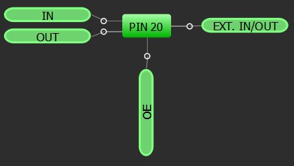
The external input/output connects to the outside of the chip to control input/output devices connected to the chip. The output enable (OE) defines if the pin is an input or output; it is an input if OE is set to ground and ouput otherwise. If configured as an input, the signal can be connected to other parts inside the chip through the IN pin (low if ground and high otherwise), and if configured as an output, the signal to the outside can be controlled by the OUT pin (low if ground and high otherwise). Additionally, the connection and resistance of the pullup resistor can be configured in the properties.
High Voltage Pins and High Voltage Control
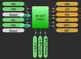
The high voltage pins work somewhat similarly to the GPIO pins, but they are controlled through the high voltage control module instead of directly, and they can only be used as an output. One thing to note is that by default, the output mode of the pin is set as Hi-Z, so to be able to drive it high or low, that must be changed in the properties. To allow the pin to be driven, the corresponding sleep must be set to ground while the corresponding output enable (OE) must be set to high. Once that's done, the corresponding IN pin can be used to control the output.
Additionally, it can be set to full bridge mode (the default is half bridge). With this, the output enable pins become disabled, so all that needs to be done to then control the output is to pull the corresponding SLEEP pins to ground. Also, the DIFF + and - pins are used for the differential amplifier with integrator and comparator and cannot be manually connected to anything.
Oscillators
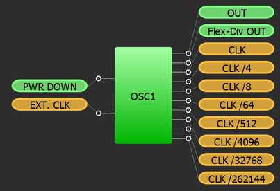
The oscillator will have a constant clock pulse that has equal time high and low. It has multiple prescalars to get different frequencies from the same clock, and each one divides the frequency of the clock by a certain amount. For example, with a prescalar of 4, it would only have a pulse every 4 clock pulses of the original, thus having a quarter the frequency. The power down pin has to be set to ground for the oscillator to be activated. The OUT pin can be manually connected to other parts of the matrix with a prescalar defined in properties while the other pins can only be connected by selecting them in the properties of other modules. The oscillator can also be configured to auto power on or force power on. With auto power on, it will only turn on if the power down pin is set to ground, AND one of the modules connected to one of the orange pins is actively using it; it will not turn on if something connecting to the OUT pin needs it. With force power on, it will turn on whenever the power down pin is set to ground. It is recommended to use auto power on to minimize power consumption and to only use force power on in testing and when absolutely necessary.
LUT
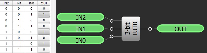
LUTs, standing for look up table, are the basic logic gates inside the ship. There are 2, 3, and 4 pin input LUTs, each with 1 output. The output states can be specified for each combination of inputs in the table in the properties by clicking on the cell in the output column to toggle the output. There are also options to set it to standard gates like and, not, and or among others.
DFF
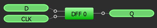
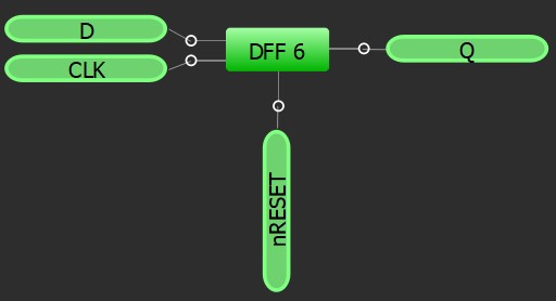
Mostly, DFFs, standing for data flip flop, come from the LUTs by changing the type in its properties. Generally, the simpler top DFF comes from the 2 bit LUT while the bottom one comes from the 3 bit LUT. The DFF will hold a constant output (Q) until the CLK line pulses (goes from low to high). Each time it pulses, the DFF will update its output (Q) to be equal to the data input line (D) until the CLK line pulses again.
In the properties, a number of things can be configured. One of the most notable is the option to invert the output, making it so that the output (Q) would instead be set to the opposite of the data input (D) at each clock pulse. Note that this would also make it so that the initial state would be high since it would invert the initial low state of the uninverted output. The initial polarity can also be changed to high to make the output high at startup.
The bottom DFF has an additional nRESET pin. By default, whenever that pin is driven low, it will reset the output to its initial state, which, as mentioned above, can be changed in the properties. In the properties, the active level for RST/SET can be changed to high to make it reset when the nRESET pin is set to high instead of low while the nSET/nRESET option can be changed to nSET to instead set the output to opposite the initial polarity.
PWM Modules
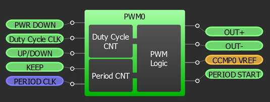
To enable the PWM module to generate a PWM signal, of course, the power down must be set to ground. The period clock is then selected in the properties; this will determine the length of the period and the frequency but not the duty cycle (i.e. the proportion of the period spent high). The output PWM signal can be taken from either the OUT+ or OUT- pin depending on if it needs to be inverted.
In addition for more control, the UP/DOWN can be connected to a signal to dynamically change the duty cycle. When connected to something, if it is driven low, the duty cycle will go down and vice versa. The KEEP pin can also be used to fix the duty cycle at the current value while it is driven high so that the duty cycle won't change no matter what the UP/DOWN pin is driven to.
Comparators
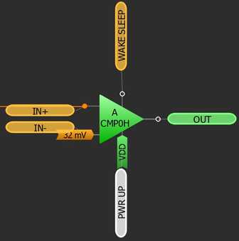
These work in the same way as every other comparator; if the input voltage is higher than the reference voltage, it outputs high and low otherwise. For these, the reference voltage is the IN- pin and is configured in properties, and the input is the IN+ pin. Of course, also PWR UP needs to be set to high for the comparator to be enabled. Additionally in properties, a gain can also be set in order to get a higher range of effective reference voltages while sacrificing precision.
Delays and Counters
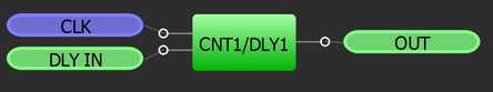
The delay counter will take an input signal and delay some amount before changing the output to match it. Whenever the input signal changes, however, even before the output updates, the counter will be reset, so it can also be used to filter out signals shorter than the delay time.
There are a variety of different properties that can be editted. Changing the counter data increases the number of clock cycles of delay there are, so if the counter data is 10, and the clock frequency is 1 kHz (1 pulse every millisecond), then the delay would be 10 milliseconds. The edge mode select can also be adjusted to choose only high or low signals to delay. If set to rising edge, it will only delay changes of the input from low to high, and the output will instantly change to low when the input changes to low. The opposite is true for falling edge, and for both edges, it will delay all changes. The output can also be inverted in the properties. The clock source can also be changed to get different scales of times, and it can also be set as external from matrix to connected it to any signal in the chip.
Blinky Example
Downloads: PCB board, Blinky configuration
Designing the Circuit Configuration
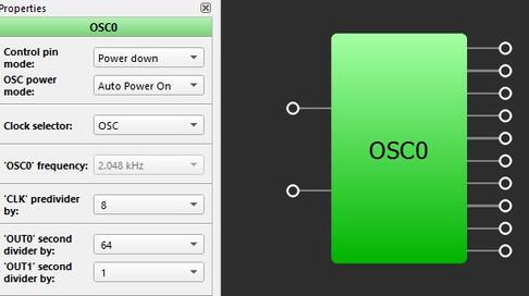
Let's start this with just a minimal blinky that just blinks without any input control. Since we want a signal to a GPIO pin that just oscillates high and low, the most straightforward thing to use is an OSC peripheral, specifically OSC0 since it has a lower frequency closer to a rate that the human eye can percieve easily. Since there is no clock selector for GPIO pins, we need to use an out pin from the oscillator. The oscillator has a frequency of 2048 Hz, so let's apply the max prescalar of 64 to the OUT0 pin, which would bring the frequency to 32 Hz, which is still a bit large. The clock to the oscillator also has a prescalar, so let's use the max prescalar of 8 for that as well. That brings the frequency to 4 Hz, which is definitely visible to the human eye, but we can bring the frequency down even futher.
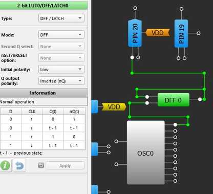
One way to use a dff is to further divide a frequency by 2. This can be done by setting the properties to invert the output and putting it back to the data input with the clock output as the oscillator output. The output of the dff would then have the half frequency to be connected to the output pin to get the half frequency to get the blinky working.
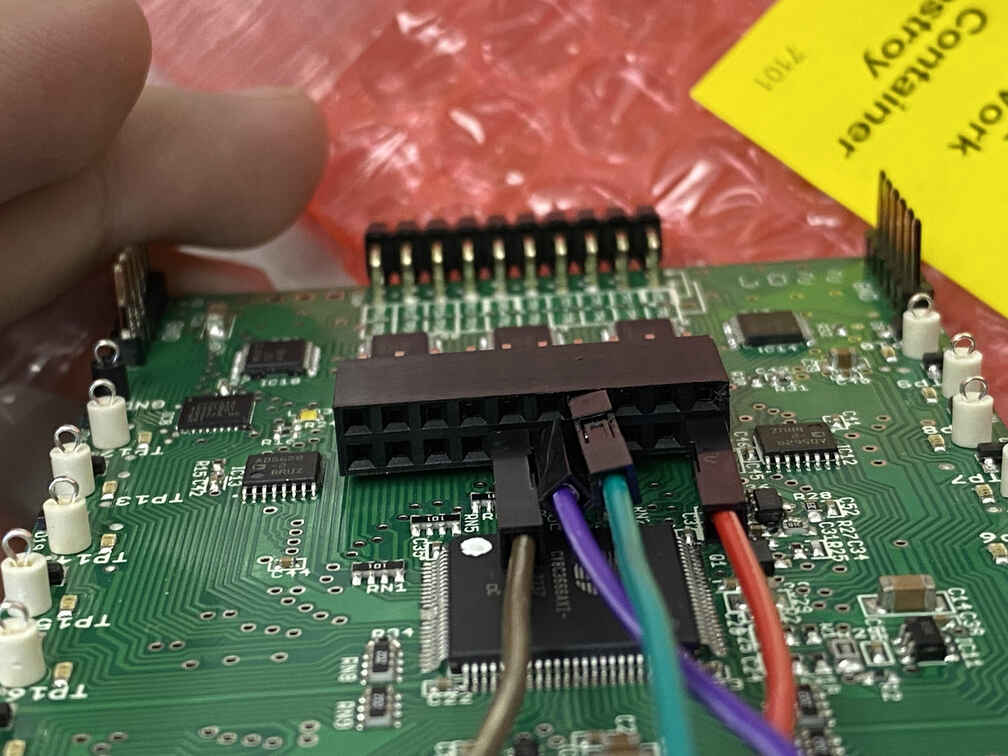
Emulation with Greenpak Advanced Dev Board
After connecting the dev board to your PC via USB, use jumper wires to connect the SDA, SCL, PWR, and GND of the dev board and the greenpak chip together according to the diagram/picture below.

Next open the debug panel in the top menue and select the GreenPAK Advance Development Platform, and hit emulate. You can also change the emulation to emulation (sync) which will update the configuration of the chip in real time as changes are made rather than needing to start and stop normal emulation for each change to the configuration.